COMPUTER POWER SUPPLY SCHEMATIC AND OPERATION THEORY
| Home | Reference | ATX3 pinout | Magnetic Units | SMPS Tutorial |
| Color Codes | Metric Conversion | Computer PSU | Calculators | ATX pinout |
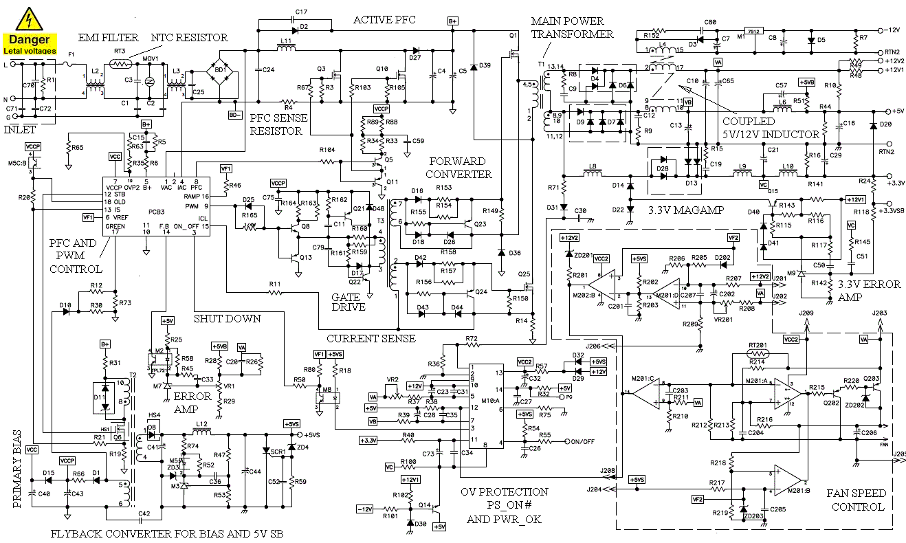
This tutorial is designed to help you better understand the operation of an SMPS. The diagram below shows a partial schematic of a 450 watt ATX power supply. Its construction is typical for a modern computer PSU with MOSFET switches and active power factor correction (PFC). Note that most schematics circulating on the internet depict old-style PSU with bipolar transistors and without PFC.
If you hover your mouse over certain sections of the drawing below you will see their brief descriptions.
 This imagemap is courtesy of Mobilefish
The AC power is applied via IEC inlet. The input current then flows via an EMI filter that reduces the level of high frequency current harmonics drawn from the mains.
Resistor RT3 limits initial inrush current into discharged capacitors C4, C5. It has a negative temperature coefficient. As it heats up, its resistance drops, which reduces conduction losses in a steady state mode.
Rectifier bridge BD1 converts bipolar AC into unipolar pulsating voltage.
Boost pre-regulator provides active power factor correction (PFC) and DC link B+ for output converter. Its power train consists of the following part: paralleled MOSFETs Q3 and Q10, inductor L11, diode D27, and storage capacitors C4 and C5.
Output converter is configured as 2-switch forward converter. Its primary section contains fast MOSFET switches Q1, Q25, and reset diodes D36, D39. When Q1 and Q25 are turned ON, DC-link voltage B+ gets applied to the primary of transformer T1. This creates positive voltages on dotted sides of all the secondaries, which in turn forward biases output rectifiers D4, D9, and after a while D28 as well.
Both MOSFETs are driven via gate drive transformer T3 with a bunch of pulse shaping components. In my view, for this power level, such a complex implementation of gate drive is absolutely unnecessary. They could just put a dual driver IC with complementary outputs on the primary side of T3 and just 10-30 Ohm resistors on the secondaries. Primary current is sensed via resistor R14. This signal is used for current mode control and power limit. The inductor L4 has three coils for +5V, +12V and -12V outputs. The coil 1-15 works in flyback mode- it conducts when Q1, Q25 are OFF.
The negative 12V voltage is regulated by a 3-terminal linear regulator M1. This power supply uses combined regulation of +5V and +12V. Error amplifier is implemented with M7, which is a 3-terminal shunt regulator, such as TL431. It senses the above rails and responds to their combination by varying current of optocouple M2, which in turn affects duty cycle of PWM. Note that since there is only one feedback point, neither output is tightly stabilized.
+3.3V rail is set by a so-called magnetic amplifier (magamp) comprised of saturable inductor L8, bipolar transistor Q15, diode D14, and control circuitry. Initial inductance of L8 is much higher than L9, so at the beginning of each switching cycle L8 prevents current from flowing through D28. Then L8 rapidly saturates and D28 begin conducting. The blocking time depends on the reset current through Q15 and D14, which in turn is set by shunt regulator M9.
The PFC pre-regulator and the main converter are controlled by an auxiliary board PCB3, whose details are not shown here.
Miscellaneous status and protection functions are implemented with IC M10. The diagram does not provide its part number. It could be a specialized monitor IC designed specifically for computer power supplies. An auxiliary flyback converter with power switch Q6 and isolation transformer T2 provides 5V standby and bias for control circuitry. It uses error amplifier M3 and feedback optocouple M5 to regulate +5VS. Finally, the circuit around quad comparator M201 provides fan speed control by using thermistor RT201.
See more schematics:
250W with active PFC;
600W power supply schematic - single-ended forward converter with passive PFC
300W legacy design with bipolar transistors (half-bridge converter);
Active PFC pre-regulator.
If you hover your mouse over certain sections of the drawing below you will see their brief descriptions.
 This imagemap is courtesy of Mobilefish
The AC power is applied via IEC inlet. The input current then flows via an EMI filter that reduces the level of high frequency current harmonics drawn from the mains.
Resistor RT3 limits initial inrush current into discharged capacitors C4, C5. It has a negative temperature coefficient. As it heats up, its resistance drops, which reduces conduction losses in a steady state mode.
Rectifier bridge BD1 converts bipolar AC into unipolar pulsating voltage.
Boost pre-regulator provides active power factor correction (PFC) and DC link B+ for output converter. Its power train consists of the following part: paralleled MOSFETs Q3 and Q10, inductor L11, diode D27, and storage capacitors C4 and C5.
Both MOSFETs are driven via gate drive transformer T3 with a bunch of pulse shaping components. In my view, for this power level, such a complex implementation of gate drive is absolutely unnecessary. They could just put a dual driver IC with complementary outputs on the primary side of T3 and just 10-30 Ohm resistors on the secondaries. Primary current is sensed via resistor R14. This signal is used for current mode control and power limit. The inductor L4 has three coils for +5V, +12V and -12V outputs. The coil 1-15 works in flyback mode- it conducts when Q1, Q25 are OFF.
The negative 12V voltage is regulated by a 3-terminal linear regulator M1. This power supply uses combined regulation of +5V and +12V. Error amplifier is implemented with M7, which is a 3-terminal shunt regulator, such as TL431. It senses the above rails and responds to their combination by varying current of optocouple M2, which in turn affects duty cycle of PWM. Note that since there is only one feedback point, neither output is tightly stabilized.
+3.3V rail is set by a so-called magnetic amplifier (magamp) comprised of saturable inductor L8, bipolar transistor Q15, diode D14, and control circuitry. Initial inductance of L8 is much higher than L9, so at the beginning of each switching cycle L8 prevents current from flowing through D28. Then L8 rapidly saturates and D28 begin conducting. The blocking time depends on the reset current through Q15 and D14, which in turn is set by shunt regulator M9.
The PFC pre-regulator and the main converter are controlled by an auxiliary board PCB3, whose details are not shown here.
Miscellaneous status and protection functions are implemented with IC M10. The diagram does not provide its part number. It could be a specialized monitor IC designed specifically for computer power supplies. An auxiliary flyback converter with power switch Q6 and isolation transformer T2 provides 5V standby and bias for control circuitry. It uses error amplifier M3 and feedback optocouple M5 to regulate +5VS. Finally, the circuit around quad comparator M201 provides fan speed control by using thermistor RT201.
See more schematics:
250W with active PFC;
600W power supply schematic - single-ended forward converter with passive PFC
300W legacy design with bipolar transistors (half-bridge converter);
Active PFC pre-regulator.